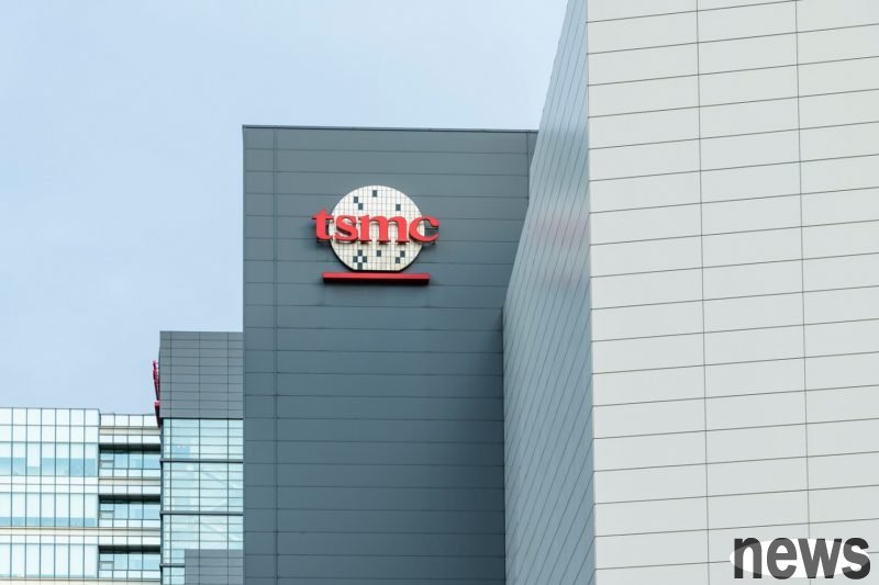
The market has been released, and the yield of NTEC's "A14" process with a ratio of 1.4 nanometers has been advanced.
Wccftech reported on the 24th that although Intel Corp.'s crystal foundry department "Intel Foundry" has announced the 14A process-related plan, there is no detailed digital performance and yield. In contrast, according to the information released by The Futurum Group semiconductor analyst Ray Wang through social platform X, the "yield performance" of the TECHNOLOG A14 process has advanced.
According to the information provided by Wang, the Telco A16 process integrates chip transistors, supercomputer (SPR) and innovative backside contact design. Compared with the N2P process, the A16 speed is increased by 8 to 10%, power consumption is reduced by 15 to 20%, and the wafer density is increased by about 1.1 times. It is very suitable for high-performance computing (HPC) products that require duplicate signal transmission and stable power supply.
$TSM‘s A16 and A14 Process Technology: “ "A14 development is progressing smoothly with yield performance ahead of schedule. " "
A16: Integrates nanosheet transists with Super Power Rail (SPR) and novel backside contacts to deliver industry-leading logic density, power… pic.twitter.com/yi9q5QPnTd
— Ray Wang (@rwang07) September 23, 2025
In comparison, the A14 completes N2 process, tailored for AI and smart phone applications, with an advanced NanoFlex Pro unit architecture.
Compared with N2, the A14 speed is increased by up to 15%, power consumption is reduced by up to 30%, and chip density is increased by more than 20%, which can bring faster computing speed, higher efficiency, and improve the AI performance of the terminal device.
According to the data provided byWang, the A14's development has been smooth, and its yield performance has exceeded the original schedule.