The team led by Professor Liu Chunsen of Fudan University successfully used the innovative ATOM2CHIP technology to directly grow a few-atom-thick two-dimensional material (molybdenum disulfide) on a traditional 0.13-micron CMOS silicon wafer, achieving a highly integrated two-dimensional NOR flash memory array combined with a standard CMOS controller. The research, published in the journal Nature on October 8 this year, marks an important milestone in two-dimensional electronics.
The success of this research means that the application of two-dimensional materials is no longer limited to laboratories. The research team reported a 94.34% yield from full-wafer testing, a figure comparable to commercial silicon wafer production and operating at speeds up to five megahertz. The energy consumption per bit is only 0.644 picojoules, which is much lower than the energy consumption of current silicon flash memory cells. The memory demonstrates fast 20 nanosecond program and erase capabilities, ten years of data retention, and over 100,000 write cycle endurance.
To achieve this result, the researchers overcame the challenge of surface roughness. Even polished silicon wafers have uneven surfaces on the nanometer scale that can tear or damage atomically thin layers. The ATOM2CHIP method introduces a conformal adhesion process that allows the 2D material to "flow" over the contours of the underlying circuitry without breaking, while a packaging system adapted to the 2D material prevents thermal and electrostatic damage.
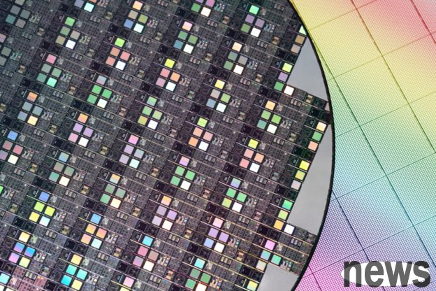
▲ A fully functional two-dimensional flash memory chip produced using ATOM2CHIP technology. (Source: paper)
In addition, the team’s “cross-platform system design” is also crucial. This custom interface ensures that the two-dimensional layer can communicate seamlessly with the CMOS control logic. This design enables instruction-driven operations, 32-bit parallel processing and random access, enabling a fully functional memory chip.
The researchers pointed out in the paper that this achievement is an important milestone in extending the advantages of two-dimensional electronics to real-life applications. Its impact is not limited to flash memory storage. If further expanded, this hybrid architecture will significantly reduce power consumption and increase the density of next-generation processors and artificial intelligence processors, thereby continuing to advance Moore's Law at the atomic limit. Although large-scale production is still several years away, this is the closest attempt to commercial application of 2D materials.
Researchers achieve breakthrough integration of 2D materials on standard silicon chips World’s First Chip Combining 2D Materials With Silicon Circuits Marks Breakthrough in Computing