
As the focus of artificial intelligence (AI) computing requirements slowly shifts from the one-time training phase to the continuous and high-frequency inference phase. This transformation not only gave rise to new chips designed for AI inference, but also brought about a revolution in heterogeneous and hierarchical architectures with "total cost of ownership" (TCO) as the core in the memory and storage fields.
As far as the field of deep learning is concerned, model training (Training) and model inference (Inference) are two completely different stages, and the two have very different requirements for graphics processing units (GPUs) and memory.
Training requires extremely high floating point computing power and high bandwidth memoryModel training is a computationally intensive task that requires extremely high floating-point computing power and high-bandwidth memory. Training, therefore, is the process by which a model learns from data, involving backpropagation, extensive computation, and multiple passes over the data set. The training workload must store the complete model parameters, and also requires a large amount of GPU memory (VRAM) to store the intermediate activations for backpropagation, the gradient of each parameter, and the optimizer state (such as Adam's first-order and second-order momentum).
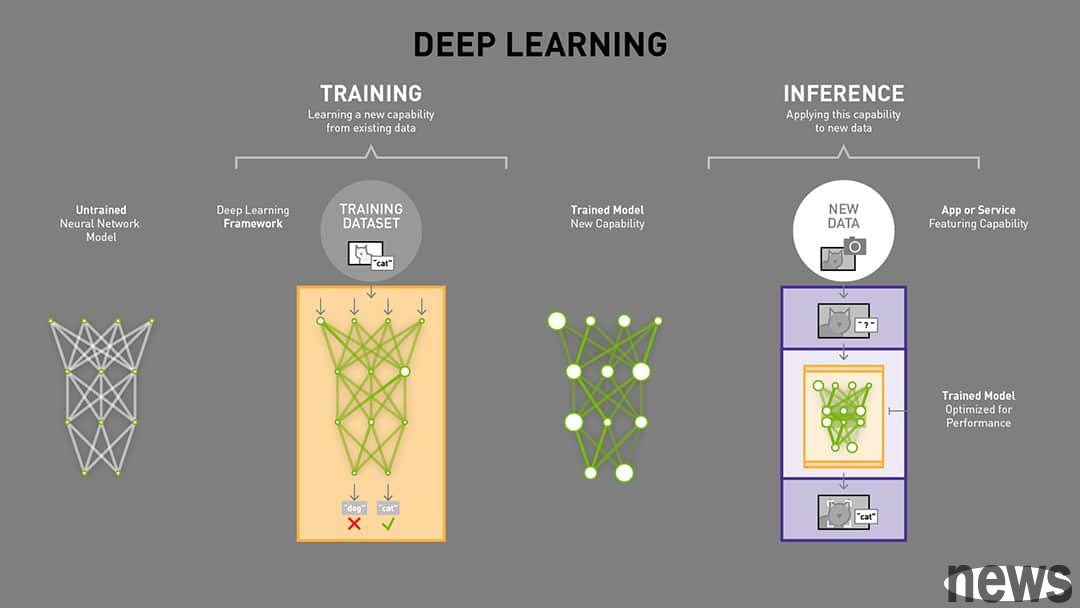
Based on the above factors, the training phase has extremely demanding requirements on memory. The model size is usually multiplied by 3-6 times the additional requirements. For example, a model with 1 billion parameters (~4 GB for FP32 weights), plus gradients (4 GB) and optimizer state (8 GB), and activations (4–16+ GB) may require a total of ~20–30 GB or more of memory. Training typically uses high-accuracy FP32 or hybrid FP16/BF16 and requires extremely high bandwidth (HBM, &>1 TB/s) because weights, activations, and gradients must be continuously accessed. Memory size is the main factor limiting the maximum batch size and trainable model size.
Inferring long scenarios focuses on fast access to large numbers of model parametersIn contrast, the model inference stage, especially long-situation tasks, although it also requires huge memory bandwidth, is more focused on fast access to a large number of model parameters. Inference is on demand, instant, and entirely shaped by user behavior, making it less of a predictable, repeatable process like training and more messy and difficult to optimize. Therefore, every user interaction with the AI—whether asking a chatbot or generating an image—triggers inference work. Inference workloads don't run in a straight line like training, they loop back, optimize, and reprocess. Each interaction triggers a large number of read, write, and lookup operations. These input/output operations per second (IOPS) quickly accumulate and put exponential pressure on the infrastructure.

In fact, “Inference = IOPS” is an accurate description of this phenomenon in the industry. The concurrent I/O driven by inference applications may even be hundreds or thousands of times greater than that of historical CPU-based computing applications. Yann LeCun, Meta’s chief AI scientist, has clearly pointed out that most of the cost of AI infrastructure is spent on inference, providing AI assistant services to billions of people. This shows that inference has become a real bottleneck in AI infrastructure.
Generative AI enters the multi-modal fusion stage, from comparing computing power to total cost of ownershipOverall, the change in AI computing requirements stems from the fact that generative AI has entered a new stage of multi-modal fusion. The core of AI applications has expanded from text-focused LLM to sound, visual and dynamic multi-modal content, such as text-generated video models such as Sora released by OpenAI. AI's move from movie generation to interactive 3D world is not only a linear increase in the amount of calculations, but also a qualitative change in calculation logic. Whether it is a movie or a 3D model, its stringent hardware requirements stem from the exponential growth in Token usage. When AI shifts from pure text to multi-modality, the number of tokens required for each video frame or 3D scene far exceeds that of text, causing the average daily token consumption to increase dozens of times in a short period of time. This explosion in demand for inference is the core driver forcing the semiconductor industry to optimize its product lines and move toward solutions designed specifically for inference workloads.
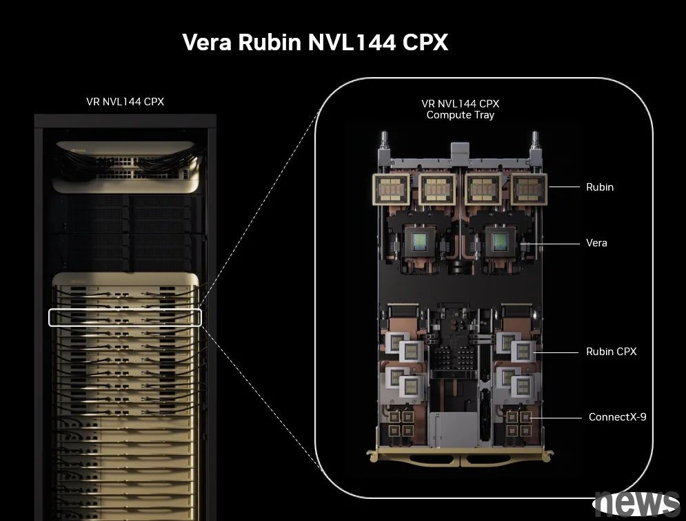
In response to the wave of inference, major semiconductor manufacturers have begun to launch solutions specifically for inference, with the goal of shifting from "computing power competition" to "total cost of ownership" (TCO) optimization. The Rubin CPX chip that NVIDIA is expected to launch is a dedicated chip designed to handle long-situation video and programming tasks. It's worth noting that Rubin CPX uses the more cost-effective GDDR7 memory instead of HBM. GDDR7 strikes the best balance between capacity, bandwidth and cost, making it suitable for inference tasks with high latency tolerance.
In addition, the inference stage can reduce memory pressure through technical means. Inference only needs to store model weights and a temporary operation buffer, and memory requirements are affected by batch size (larger batches have more activation values). Inference can use quantization technology, using INT8, FP8 or even 4-bit quantization, to significantly reduce memory usage and bandwidth requirements. For example, after quantization optimization, a 7 billion parameter model that originally required 16 bits can be compressed to 4 bits and run inference on an 8GB GPU. This makes inference much more memory efficient than training.
Artificial intelligence demand market development impacts memory solution challenges and changesAs AI models become increasingly larger, existing memory solutions face challenges. Although HBM has extremely high bandwidth but limited capacity, eSSD has huge capacity but insufficient bandwidth and latency. AI inference requires high IOPS, so the storage system must keep up with the speed of computing, otherwise the fastest computing architecture will be of no use.
The rise of enterprise-class SSD and out-of-stock warningIn the data processing of AI servers, the pursuit of high IOPS has caused enterprise-class solid-state drives (eSSD) to accelerate the replacement of traditional hard disks (HDD). Although the unit cost of eSSD is higher, with the advancement of QLC technology, its cost per GB has been significantly reduced, and the price difference with HDD has narrowed. The access speed of eSSD is much higher than that of HDD.
Cloud service providers are actively planning to replace HDDs with eSSDs on a large scale in 2026, which will trigger a surge in demand for large-capacity QLC SSDs and may lead to "serious shortages" in 2026. This signals that the growth engine of the NAND market is shifting from traditional consumer products to enterprise-class storage.
The emergence of high-bandwidth flash memory (HBF)To bridge the gap between HBM and eSSD, SanDisk and SK Hynix are collaborating to promote high-bandwidth flash memory (HBF). HBF is strategically positioned to provide a solution that combines high capacity with high bandwidth, making it ideal for inference on very large AI models.
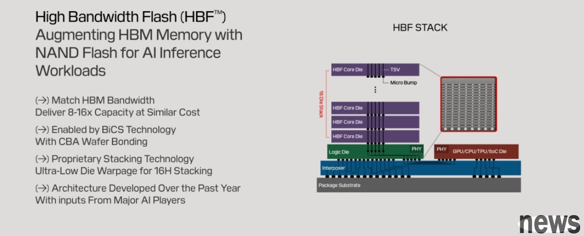
HBF 3D stacks NAND chips and directly connects to the GPU through through silicon through holes (TSV). HBF is expected to have bandwidth comparable to HBM, but have 8 to 16 times the capacity. This innovation indicates that the AI memory architecture is forming a new three-tier system, including HBM as the high-speed cache layer, HBF as the large-capacity model storage layer, and eSSD as the underlying data lake.
Edge AI and NOR Flash OpportunitiesAI’s impact on memory is not limited to cloud data centers. As AI technology is pushed from the cloud to terminal devices such as AI headsets, AI glasses, and AI PCs, the importance of edge computing has become increasingly prominent. In these edge AI applications, NOR Flash becomes a key component. Because the memory cells of NOR Flash are designed in parallel, they have excellent random access capabilities and extremely fast reading speeds, and allow program codes to be executed directly within the chip (eXecute In Place, XiP). This makes it ideal for storing activation code, firmware and critical code in edge AI devices.
The golden age and strategic layout of the memory industry chainThe explosive growth in demand for AI inference is consuming memory production capacity at an unprecedented rate, resulting in an imbalance between supply and demand in the DRAM and NAND flash memory markets.
This wave directly boosted the demand for HBM and DDR5, and spread to the entire industry with a "ripple effect". Several Wall Street institutions predict that, supported by strong demand for AI, the world's key memories will face supply shortages in 2026, and contract prices for DRAM and NAND flash memory are expected to continue to rise in 2025 and 2026. The growth in enterprise-class SSD shipments has also boosted the overall NAND industry revenue.
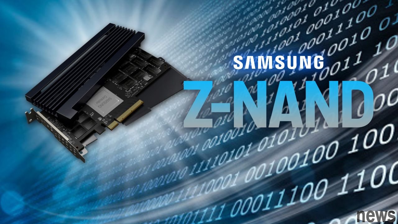
As AI drives a surge in demand for HBM, various manufacturers are actively developing alternative technologies to balance performance, power consumption and cost. First, Samsung announced the restart of Z-NAND and the introduction of GPU pass-through access (GIDS), which allows the GPU to directly read stored data, eliminates CPU/DRAM bottlenecks, and improves LLM and HPC training efficiency. The new generation of Z-NAND will have 15 times the performance of traditional NAND and reduce power consumption by 80%, continuing the technical foundation of the 2018 SZ985 Z-SSD.
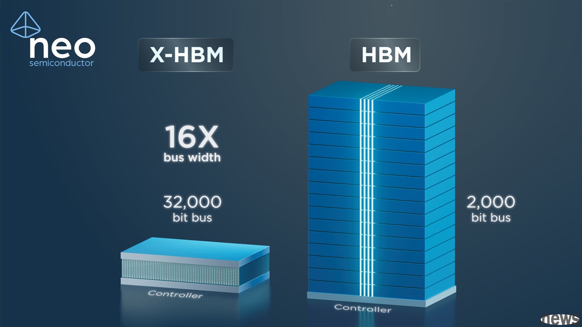
Secondly, NEO Semiconductor launched the X-HBM architecture, using 3D X-DRAM to break through the HBM bandwidth and capacity limitations. Its single chip capacity reaches 512Gbit, the data bus is 32K-bit, and its bandwidth and density are 16 times and 10 times that of the existing technology respectively, far exceeding the expected HBM5 in 2030 and HBM8 in 2040. There is also Saimemory, which was founded by SoftBank, Intel and the University of Tokyo. It focuses on stacking DRAM and combines Intel EMIB technology to achieve twice the capacity and 40% to 50% lower power consumption than HBM. The cost is also more advantageous. It plans to complete the prototype in 2027 and commercialize it in 2030, focusing on green computing.
Finally, SanDisk and SK Hynix are collaborating to develop high-bandwidth flash memory (HBF), which combines the non-volatile characteristics of NAND and HBM packaging. The capacity is 8 to 16 times that of DRAM-type HBM. The cost is lower but the delay is slightly increased. Samples are expected to be launched in 2026 and applied to AI inference equipment in 2027. Overall, these solutions each emphasize bandwidth breakthroughs, energy efficiency optimization, or cost reduction, representing that the industry is exploring new paths for AI memory beyond HBM.
In the future, the development of AI memory will revolve around the hierarchical storage architecture. A new system is being formed consisting of HBM as the high-speed cache layer, HBF as the large-capacity model storage layer, and eSSD as the underlying data lake. Or, build a new storage architecture through the development of new storage products and technologies. In particular, AI inference's extremely high requirements for IOPS have elevated storage systems to the status of core infrastructure. This hardware revolution in computing and storage has just begun. Companies that can discern and plan for this change will undoubtedly take the lead in the new era of AI.